

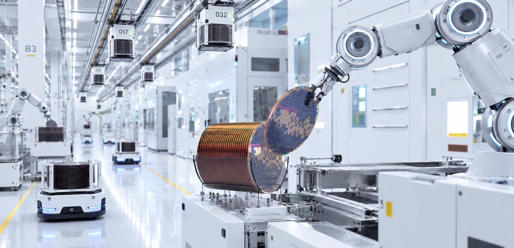
SEMICON is one of those events that lets you step into the world of the future. It disengages you from the present and shows what the semiconductor industry will look like a few years from now.
And the main look of that future is: bigger, richer, and more efficient.
SEMICON Taiwan, specifically, lets you specially enter the physical world of semiconductors: the actual machinery, materials, and processes being used to turn rocks into computational power and, ultimately, intelligence.
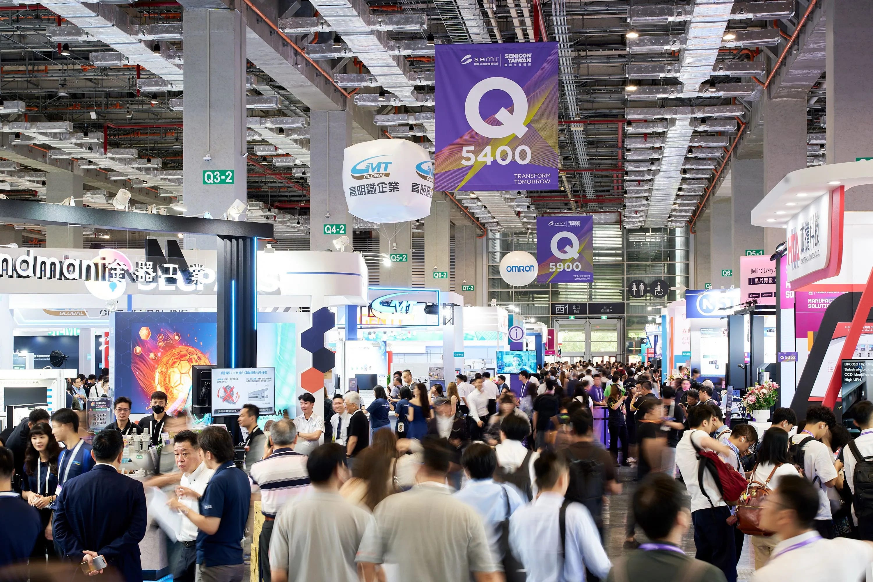
This year, the excitement was palpable, and I dare to say it was the most excited the semiconductor public has felt since, probably, forever.
The reason why is obvious: AI is injecting so much money into this industry that not only are growth, earnings, and stock prices soaring, but funding for new technologies has skyrocketed.
This is accelerating progress like never seen before.
This can be seen in the development roadmaps of large companies like AMD or Nvidia. Going from one generation every three years to a new generation yearly, sometimes even with a completely new architecture per year, is simply out of this world.
Scaling performance by orders of magnitude, sometimes just within a frequency of months, would have been absurd when the industry was solely dependent on Moore’s Law. Today, the industry is making all these metrics explode through implementing advanced packaging techniques that are making systems larger and more powerful than ever.
And this was the most popular and consequential theme of the event.
Yes, it wasn’t photonics, memory, or the logic die itself. It wasn’t design or foundry.
It was advanced packaging.
The reason? All of the above depends on it.
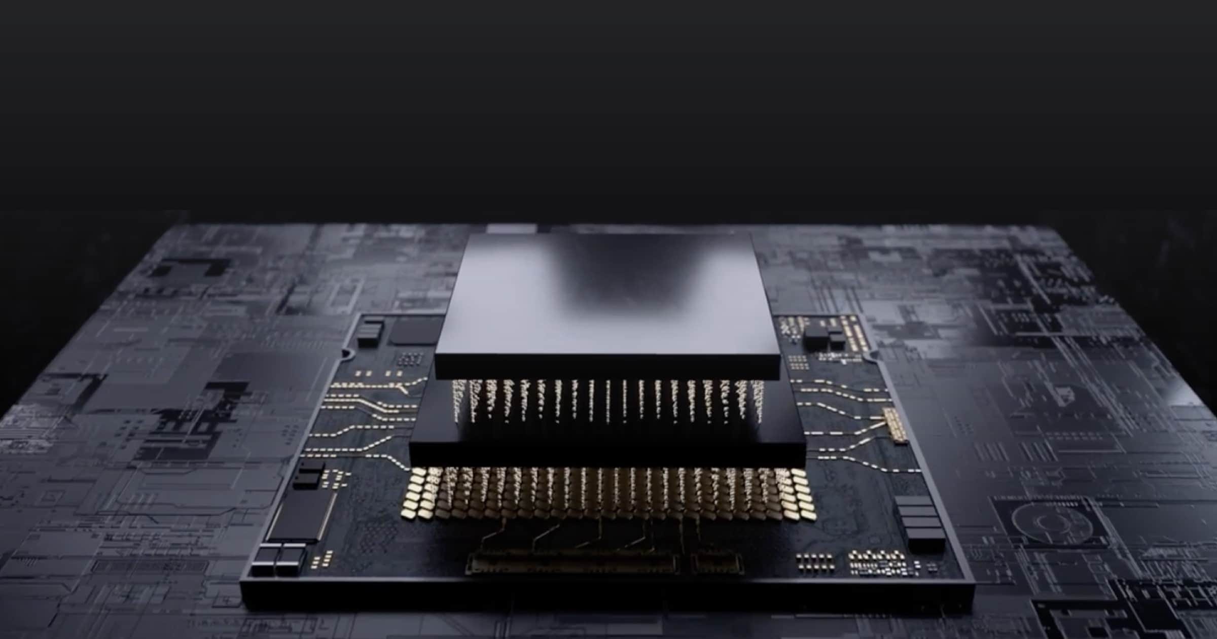
You can’t build a CPO switch without advanced packaging, you can’t stack more layers of HBM without advanced packaging, and you can’t scale logic dies in bigger and bigger world sizes without advanced packaging.
Since increasing the density of transistors is increasingly challenging, advanced packaging is, and will increasingly be, the defining scaling anchor for compute and, ultimately, of the AI era.
What were the attendees, from engineers to analysts, sales teams, and journalists, more interested in?
The core of the event was Fan-Out Panel-Level Packaging.
The nascent star: glass substrates.
And the satellites supporting these technologies: robotics, specialized machinery that scales well beyond wafers, and advanced materials that make the transition toward these new technologies, including hybrid bonding, possible.
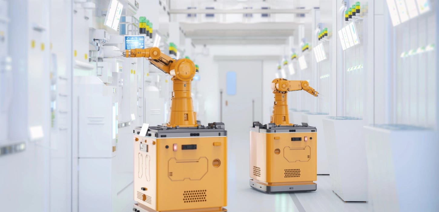
To take advantage of this opportunity in the semiconductor space, I’ll initiate a new series where I’ll be dissecting the companies that supply companies like TSMC, Intel, Micron, and Samsung, including complex automated machinery and robots that transport the key components manufactured in a fab, so that investors know how to get exposure to these companies’ expansion plans.
I’ll consider not just the technology, which is the core aspect, but also the financials and valuations.