
Semiconductor Bottlenecks and Stocks
Bottlenecks and companies solving them, bullish and bearish trends, and stock ideas

There are many ways to play the AI boom
In the full article, I cover:
All the main bottlenecks, including these and more
The companies solving those bottlenecks
Bullish and bearish themes and stocks
Where the industry is heading and which companies are leading
Valuation models and stock price targets
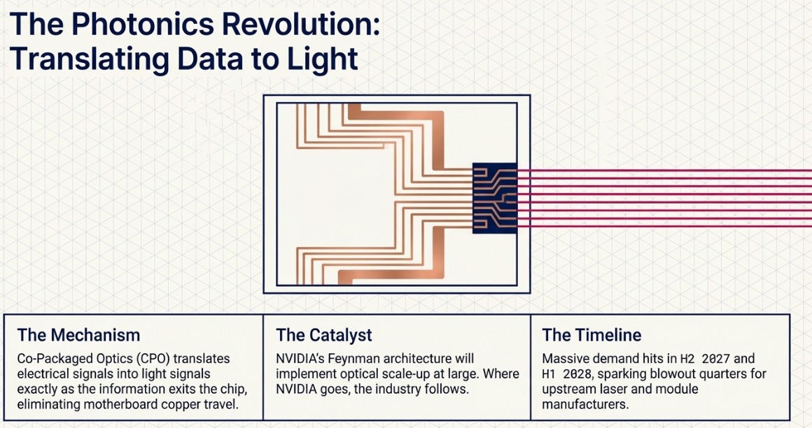
Photonics
One of the most at-the-edge opportunities is CPO and the broader scale-up architectures that will emerge over the next few years.
For anyone interested in learning more about this, I recommend my article on optical networking stocks.
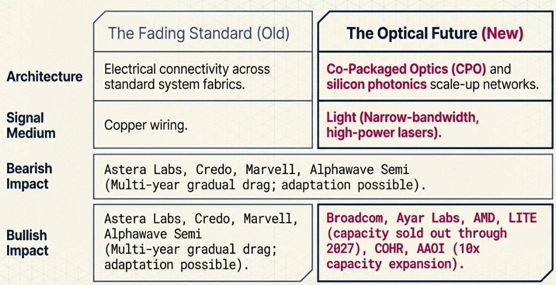
As a summary, CPO consists of translating electrical signals into light signals just as the information exits the chip, while optical scale-up networking consists of moving that optical connectivity beyond the package and across the broader system fabric. This involves a technology called silicon photonics, which integrates optical components directly onto silicon to enable much faster, more power-efficient data movement at scale.
The demand is going to grow exponentially. LITE is currently sold out in its high-power narrow-bandwidth lasers through the end of 2027, COHR is painting a similar picture, and AAOI is expanding its capacity by 10x to meet demand. Most of this demand will hit in H2 2027 and H1 2028, which is when you will start seeing blowout quarters for these companies. This is because the first architecture to implement optical scale-up will be NVIDIA’s Feynman, and where NVIDIA goes, the rest follow. So we will likely see even more demand than expected as other players like Broadcom, which also has in-house laser manufacturing capacity, Marvell, Ayar Labs, AMD, and others join the CPO race.
Overall, this change in architecture is bearish for companies deeply embedded in the old connectivity architecture, such as Astera Labs, Credo, Marvell, or Alphawave Semi, now acquired by Qualcomm. When I say bearish, I mean on a multi-year basis, and the fact that it is bearish does not mean these companies will necessarily do badly. Even if at the macro level the new paradigm is worse for them, the shift will be gradual, and there is even a chance these companies will adapt.
In fact, they are already making efforts to try to do so.
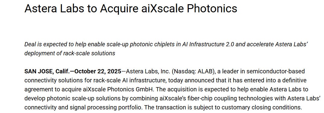
Astera Labs
Astera Labs acquired aiXscale Photonics in October of last year. aiXscale brings fiber-chip coupling and optical I/O precision glass coupler technology, which is used to connect photonic integrated circuits to optical fibers in dense systems. Astera said this should help it build photonic chiplets and photonic scale-up solutions for rack-scale AI.
Pivoting from retimers to scale-up optics is not an easy task, but these companies need to justify their terminal growth assumptions to analysts. Optical scale-up is inevitable, and Astera has built a business around a technology that will slowly be replaced.
In January 2026, Astera also said its Scorpio X-Series roadmap would add optical connectivity, including photonic switch-to-accelerator links for multi-rack deployments that could scale to thousands of GPUs. In December 2025, Astera also said its new custom connectivity offering would benefit from its newly acquired photonic chiplet technology.
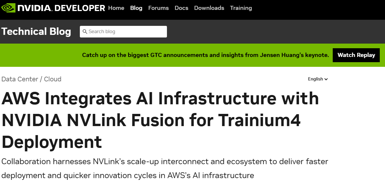
This may sound good. However, as I covered before, Astera’s largest customer, Amazon, has co-adopted NVLink Fusion for Trainium4, which lowers the chances of Astera Labs keeping such high volume inside Amazon’s racks.
Moreover, Astera Labs was left out of ESUN, a new open-source architecture backed by Meta, AMD, Broadcom, Marvell, and others, which strongly suggests there will be market share erosion from Broadcom and Marvell.
Marvell
As we saw before, Marvell acquired Celestial, which gives it a first-class pass into the optical scale-up ecosystem.
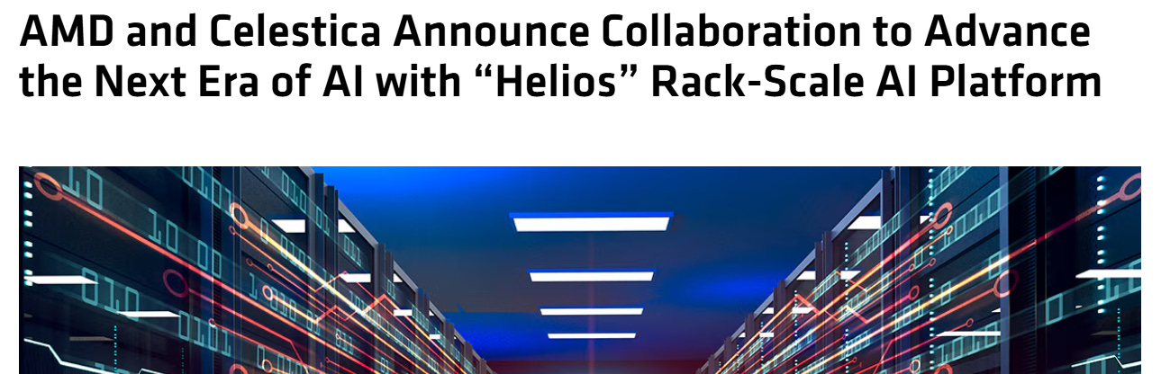
Celestial is one of the top silicon photonics companies for scale-up, and it already has an important partnership with AMD to develop optical scale-up solutions for next-generation architectures.
Credo

Credo acquired Hyperlume in September 2025 to add microLED technology to its connectivity portfolio for future AI data infrastructure, although the credibility of this technology is still at a very early stage.
Qualcomm
Qualcomm acquired Alphawave Semi, which had already been expanding into optics for some time, mostly into 800G and 1.6T DSPs.

Qualcomm has opted for partnerships, collaborating with Lightmatter in a co-packaged optics reference architecture initiative.
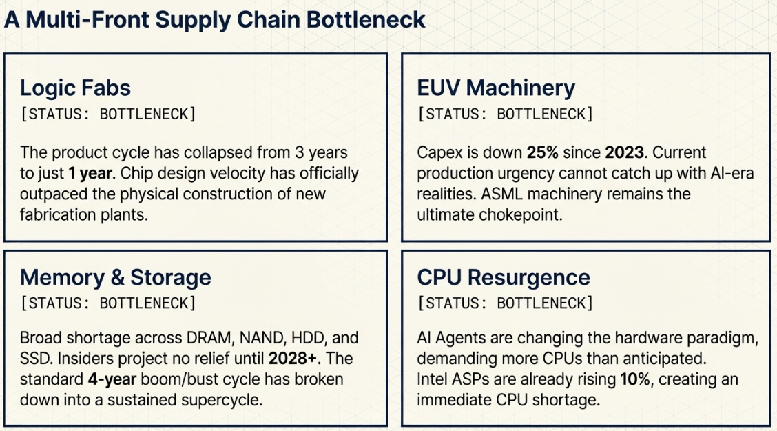
Logic fab shortage
We are already in a logic fab shortage, but the product cycle is shortening from 3 years to just 1 year. You can design better chips in today’s world than you can build new fabs, which will inevitably create one of the biggest bottlenecks.
There is also an expected EUV machine shortage. It all comes down to EUV machines, and with ASML not showing too much urgency around expanding its CAPEX efforts, with capex down 25% since 2023, it is hard to see production of these machines catching up with the reality of the AI era.
Memory shortage
There is also a memory and storage shortage. Anywhere you look, whether DRAM, NAND, HDD, or SSD, there is a shortage. From insiders, we know this will not end until 2028 at the earliest. No one knows what advancements in AI we will get by then. Some will probably be extraordinary, and we may never get memory relief at all. Although it sounds extreme to say it, this time may actually be different, and we may not get the usual boom and bust cycle.
I’m heavily invested in Micron. For the moment, everything points toward a continuation of what we’ve seen, although I would not be opposed to diversifying my semi exposure into other, less crowded names.
CPU shortage
A CPU shortage is another part of this story. Agents are changing the landscape. As Lisa Su said at a recent event, hyperscalers and AI labs are surprised to see that agents can perform better with more CPUs. This changes the paradigm.
Up until now, the consensus was that AI would gradually shift demand for CPUs toward GPUs. Now, it may seem that, as Lisa has always said, there is not one solution that fits all needs, and in the case of agents, CPUs are needed more than for other purposes. This is creating a CPU shortage for this very same year.
That is very beneficial for AMD, and it could become extremely beneficial for Intel, especially if it can successfully convert its foundry capacity toward more data center products. Its new Panther Lake retail CPU is great, but the margins will not be anywhere near as good as what it could get from data center chips, especially considering it is made on its 18A process.
NVIDIA is going to be another beneficiary. In fact, at the latest GTC, Jensen said they are now offering CPU-only racks and that he sees this becoming a multi-billion-dollar business by itself.
Advanced packaging
Advanced packaging is another example, especially 2.5D + HBM integration, which is currently in a bottleneck.
NVIDIA’s Jensen Huang said in January 2025 that advanced packaging capacity had quadrupled in under two years and was still a production bottleneck. TSMC then said in April 2025 that CoWoS demand was still above supply even while it was doubling capacity, said again in July 2025 that it was still trying hard to narrow the gap for 2025 and 2026, and in January 2026 was still talking about narrowing its demand-supply gap while raising advanced-packaging-related investment.
Intel is also stepping in to help solve the bottleneck with EMIB-T, a 2.5D bridge packaging technology designed mainly for very large AI and HPC packages that need tighter HBM4 integration, faster die-to-die communication, and better power delivery. Intel is now working on improving EMIB and EMIB-T yield and quality to support customer ramps beginning in the second half of 2026.
Intel is partnered with Amkor, which is the main assembly and scaling partner for the broader EMIB ecosystem, while Synopsys, Cadence, Keysight, and Siemens are the main design and validation partners helping customers build around EMIB-T. Intel has also shown proof-of-concept work with Trusted Semiconductor Solutions using EMIB-T for 2.5D assemblies with a path toward 3D through Foveros.
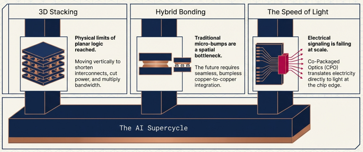
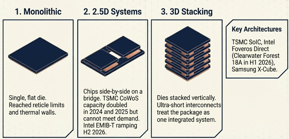
3D packaging
3D packaging is the next step in the advanced packaging roadmap. The industry first moved from big monolithic dies toward advanced packaging, then toward 2.5D systems like interposers and bridges for chiplets plus HBM, and the next step is 3D stacking, where dies are placed vertically to shorten interconnect length even further, cut power, and increase bandwidth.
Foveros Direct is Intel’s 3D packaging technology. It works by stacking chiplets on an active base die using direct copper-to-copper hybrid bonding, with ultra-high-density die-to-die links aimed at better bandwidth and lower power per bit. Instead of placing dies only side by side and connecting them with a bridge like EMIB, Intel can stack one die directly on top of another and treat the package more like one integrated system.
Clearwater Forest will combine Intel 18A, Foveros Direct 3D, and EMIB 3.5D, with launch timing in the first half of 2026.
TSMC’s CoWoS is a 2.5D solution that dominates today’s AI accelerator packaging, and SoIC is TSMC’s 3D silicon stacking technology.
SoIC entered mass production in 2023 to support customers’ next-generation flagship AI products. However, the bottleneck has been in CoWoS, where demand is still greater, although it seems like that could change soon. In January 2024, TSMC said advanced-packaging demand was so strong that it was doubling CoWoS output in 2024 and still could not fully support customers. In April 2025, TSMC said it had to double CoWoS capacity again, that it was still fully loaded, and that 2025 would probably be mostly CoWoS-S, while 2026 would move more toward CoWoS-L. In that same April 2025 call, TSMC said customers were starting to pick up SoIC and more advanced packaging technologies, which tells you SoIC is moving from roadmap to adoption, but it was still not the main volume engine yet.
Samsung’s 3D packaging technology is X-Cube, which works by stacking logic dies vertically. The most advanced version will use hybrid copper bonding, with 4 µm-pitch hybrid copper bonding coming in 2026.
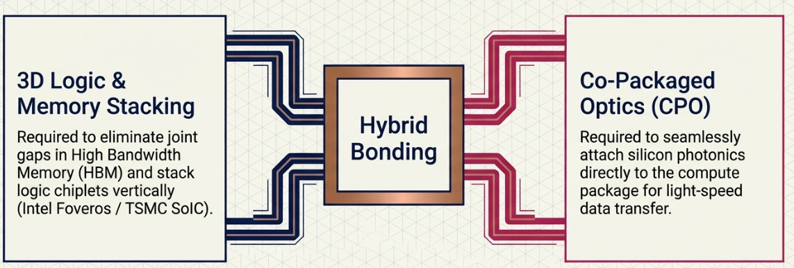
Hybrid bonding
Hybrid bonding is one of the key technologies behind 3D packaging.
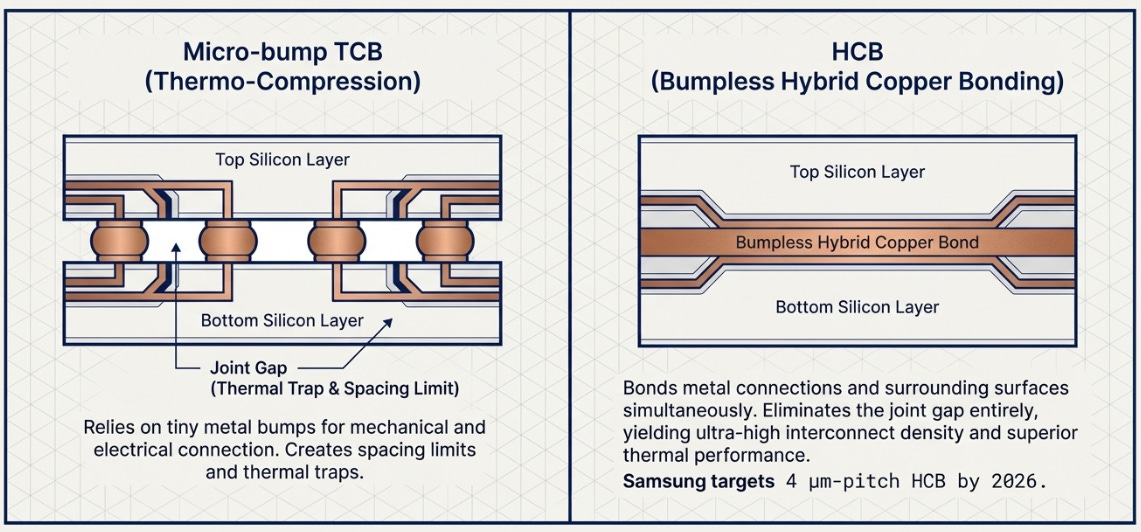
There will be an inevitable hybrid bonding boom, replacing the old thermo-compression bonding, or TCB, with hybrid copper bonding, or HCB.
BESI supplies assembly, die attach, and hybrid bonding equipment used in semiconductor packaging.
Micro-bump TCB bonds tiny metal bumps between two dies. Those bumps make the electrical connection and the mechanical attachment.
Hybrid bonding bonds copper to copper, plus the dielectric surfaces around them. That is why it is called hybrid: you are bonding both the metal connections and the surrounding surface together.
According to Samsung, bumpless hybrid copper bonding provides much higher interconnect density and thermal performance by eliminating the joint gap.
The problem for BESI is that management expected the higher-priced, less competitive, higher-margin hybrid bonding business to become its largest assembly segment by 2030, based on the assumption of a shift from TCB to hybrid bonding in HBM5. Meanwhile, according to a reported consensus from the last JEDEC meeting, which sets the industry standards body for memory and semiconductor interfaces, standardization for HBM could get delayed from 2030 to HBM6 in 2032, which would hit BESI’s expectations.
However, the BESI bull thesis goes beyond that.
Hybrid bonding is also used for co-packaged optics, which will start proliferating in data center architectures this year and become standardized in bleeding-edge deployments throughout the decade.
In fact, photonics may be a bigger opportunity for BESI overall than memory, because BESI also sells other tools for photonics, like its multi-module attach platforms.
Photonic foundry capacity
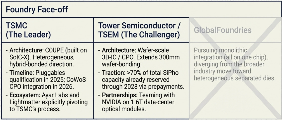
If there is a photonics shortage, and CPO usage is going to explode, it is natural to look upstream, and that is where the photonic foundries sit.
The two main players here are TSMC as the leader and Tower Semiconductor (TSEM) as a very credible second. Tower said in February 2026 that more than 70% of its total SiPho capacity is already reserved, or in the process of being reserved, through 2028, backed by customer prepayments. That speaks to the bottleneck, and it is reminiscent of the one in memory.
Although we do not have demand figures from TSMC, it is the leader through its COUPE architecture, so this will likely become a significant segment for it through the next decade.
GFS wants to position itself as a significant player in SiPho. However, GF is pushing a monolithic silicon photonics model, meaning the CMOS/RF electronics and photonic devices are integrated on the same chip. However, the industry is moving in a different direction.
TSMC COUPE uses SoIC-X and is built to bring optics directly into the package, first with pluggables qualification in 2025 and then CoWoS CPO integration in 2026. That is a heterogeneous, hybrid-bonded direction, where the photonic die and the electrical die are separated and then integrated more tightly.
For example, Ayar had a long history with GF, with GF itself saying the two had been collaborating since 2016 on a monolithic in-package optical interconnect approach. However, more recently Ayar has been publicly disclosing that it is clearly aligned with the TSMC ecosystem, as its 2025 announcement with Alchip explicitly tied its optical engine roadmap to TSMC advanced packaging and process technologies.
Lightmatter made that direction even more explicit in January 2026, saying Synopsys was adapting 224G SerDes and UCIe IP for TSMC’s COUPE process, specifically to make it hybrid-bond compatible for Passage.
Tower’s newer offering is not monolithic either. In November 2025, Tower announced a wafer-scale 3D-IC / CPO foundry technology that extends its existing 300 mm wafer-bonding capability to enable heterogeneous integration across its SiPho and SiGe BiCMOS platforms, moving toward the same broader industry direction of separating the photonic and electronic functions and then integrating them more tightly, rather than insisting everything must live on one monolithic die.
Tower is also building more credibility in SiPho than GF. In 2025, Tower and Innolight said they were expanding their collaboration on Tower’s newest SiPho platform, which Tower described as already in production and ramping to high volume for AI and data-center optical modules. In February 2026, Tower announced it was teaming with NVIDIA on 1.6T data-center optical modules designed for NVIDIA networking protocols. Other partners include OpenLight, NewPhotonics, Scintil, Salience, Oriole, Xscape, LightIC, Lightwave, and Xanadu.
Sometimes it is hard to get a grip on how big these opportunities can be. You can say X or Y is a leader in an important part of the supply chain, but that is not enough of an investment thesis.
You need to factor in valuations.
Some companies have given us some insight into what their future could look like, which is what I’m going to focus on primarily in this particular article.
Company-by-company analysis
Keep reading with a 7-day free trial
Subscribe to Daniel Romero to keep reading this post and get 7 days of free access to the full post archives.